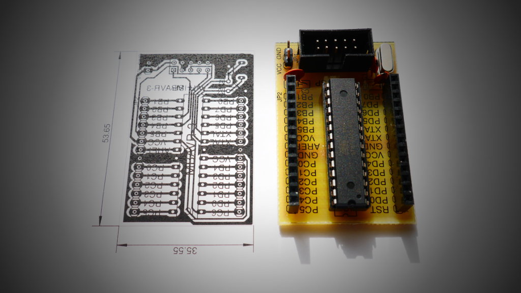
This is another quick how-to guide of making a minimalist development board for AVR. This time is about MBAVR-3 development board designed for megaAVR MCUs like ATmega8, ATmega88, ATmega168 or ATmega328. It is a 3rd project in series of MBAVR familly home-made boards in order to create an nice environment for rapid development. I did these things at home. I used toner transfer technique to make both PCB layers. I’m very pleased with the results.
Intro
The project goal was the same as of previous version (2) – to create minimalist development board that will:
- base on signle-layer PCB layout,
- include only through hole parts,
- expose AVR ISP socket (JP3) for USBasp programmer,
- make all GPIO pins available on the PCB via headers (JP1, JP2)
- contain MCU socket and extra power connector (JP4).
Designing complex development boards is often overkill, especially when you want it small size. On the board shown here, I’m only using the features turned out to be handy for what I’m using in my projects. I focused on design that in my opinion is possibly a simplest, smallest, and cheapest.
List of elements:
- PCB,
- microcontroller (ATmega8/ATmega88/ATmega168/ATmega328),
- DIL-28 socket,
- two pin headers 14×1,
- and one pin header 2×1,
- crystal 16Mhz,
- two capacitors 22pF,
- capacitor 10nF (decoupling capacitor).
Diagram Circuit
Additional information about schematic and PCB can be found in eagle project which is attached to this article as a zip file.


Hi
I want to buy PCB of atmega8 ISP.
Hi there. Quick query – your schematic appears to have connected all 4 GND and the VCC pin of the ISP connector to GND, and JP4 appears to short GND and VCC – is that what you intended? The PCB bottom layout shows the ISP VCC and GND as separate, but there is still the option for shorting VCC to GND via JP4 if I understand correctly?
Hi Kevin, the order of pins in used eagle element (AVR-ISP socket) on schematic is not 1:1 what you see on PCB. The second thing – it’s not a jupmer but a pin header to connect external power supply, i.e. battery. Not for shorting VCC and GND. Anyway, it was not my intention to treat it as jumper.
Hi,
Have you plan your PCB ?