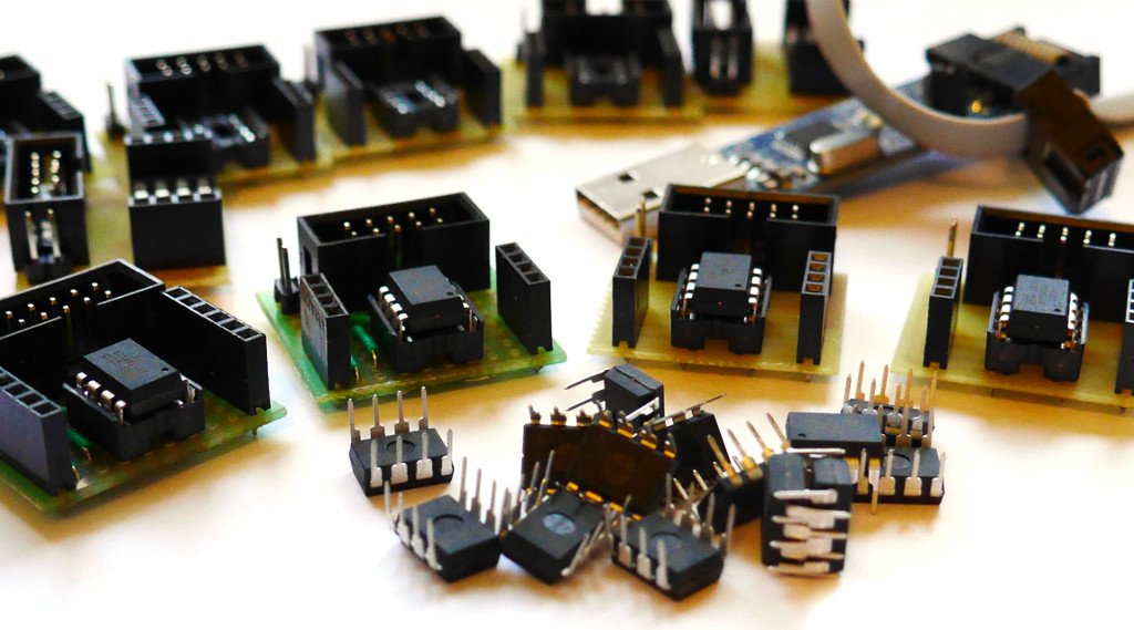
This is a quick how-to guide of making a minimalist development boards for MCU of tinyAVR family like ATiny13/25/45/85. The idea behind this project was to create an environment for rapid development. I’ve been designing many projects based on this little MCUs and I didn’t want to wire it all up any more by hand. Next reason is that all of the AVRs I use in a package DIP-8 share the same ISP connector pinouts. And finally, due to many of my projects available on this website are based on this little board, I’m going to explain how it works and how you can do it yourself at home.
New version available! ⇒ https://blog.podkalicki.pl/avr-development-board-for-attiny13-attiny85-etc/
1. Intro
The project goal was to create minimalist development board that will:
- base on signle-layer PCB layout,
- include only through hole parts,
- expose AVR ISP socket (JP1) for USB ISP programmer,
- make all GPIO pins available on the PCB via headers (SV1, SV2),
- contain MCU socket and extra power connector (JP2).
Designing complex development boards is often overkill. In the board shown here, I’m only using the features turned out to be handy for what I’m using in my projects. I focused on design that is possibly a simplest, smallest, and cheapest.
List of elements:
- PCB,
- microcontroller (ATtiny13/25/45/85),
- DIL-8 socket,
- two pin headers 4×1,
- and one pin header 2×1.
2. Schematic & PCB
I will not provide information about how to make a printed PCB because it’s a part of different topic but there are at least two ways of how you can do it at home – please, take a look here. Any additional information about schematic and PCB can be found in eagle project which is attached to this article as zip file.
3. Board assembling
Assembling boils down to placing these few components on the PCB and soldering them. Piece of cake!
4. Protoboard as an alternate version of PCB
Because of our circuit is pretty simple – just a few parts, low frequency and low current – our requirements for traces of PCB are also correspondingly smaller. It means that an approach of using protoboard is fully acceptable. So, here is an example of how we can easly wire it up using perfboard (“pad-per-hole” type of protoboard). There are three common methods of wiring on the protoboards – using jumper wire, solder bridges and using leads. In presented example two of them has been used – wire leads from the bottom and jumper wires on the top. Here is what I ended with.
5. Summary
If you made it, then congrats – you have a very nice minimalist development board ready to use! So where do you go from here? First, get that USBasp programmer if you haven’t already got one and then start with “blinky” projects. There’s no shortage of interesting AVR projects on this website 😉 If you’re a beginner I also recommend read this


Brak kondensatorów na płytce…
Zaleca się oczywiście, żeby były kondensatory ale w tej minimalistycznej wersji (MBAVR-1) celowo je pominąłem. Wynika to głównie z faktu, że przez wiele lat używałem podobnej konstrukcji do budowania prototypów i nie spotkałem się z problemami.