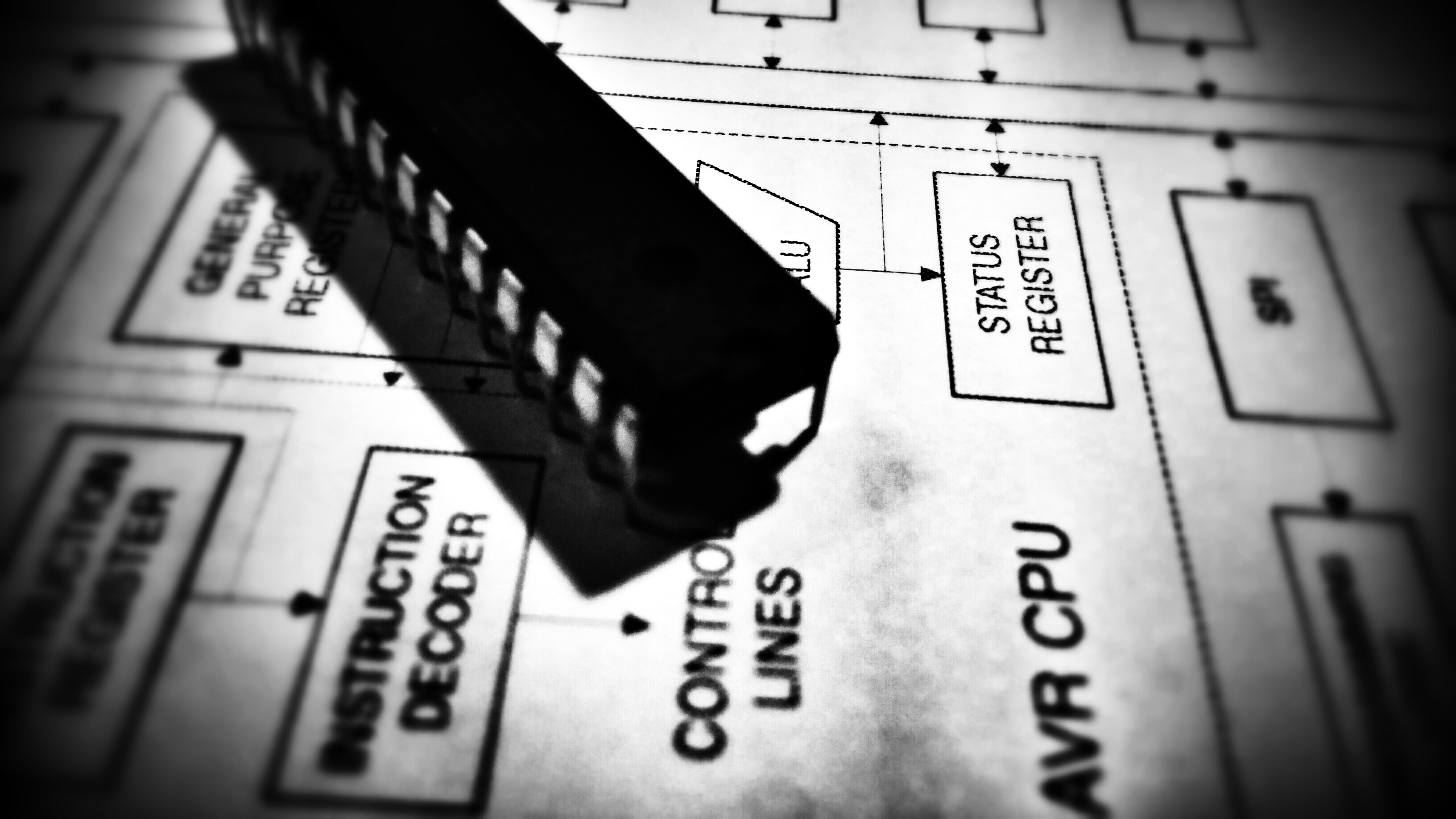
The AVR architecture is a huge topic in itself. I will just provide a general picture of how the AVR microcontroller works. The AVR uses a Harvard architecture thus it has separate memories and buses for program and data. Instructions in the program memory are executed with a single level pipelining. While one instruction is being executed, the next instruction is pre-fetched from the program memory. This concept enables instructions to be executed in every clock cycle and that imply AVR runs at around 1 MIPS / MHz.
Block Diagram
CPU
The AVR’s CPU is similar but much simpler like the one in a computer. The main function of the CPU is to ensure correct program execution. The CPU must therefore be able to access memories, perform calculations, control peripherals and handle interrupts. Atmel’s 8- and 32-bit AVR CPUs are based on an advanced Harvard architecture thus every chip has two busses – one instruction bus where the CPU reads executable instructions and one data bus to read or write the corresponding data. The AVR’s CPU core consists of :
- ALU – short for Arithmetic Logic Unit, supports arithmetic and logic operations between registers or between a constant and a register. After an operation is executed, the Status Register is updated to reflect information about the result of the operation.
- General Purpose Registers – Register File that contains 32 x 8-bit general purpose working registers. All registers have single clock cycle access time what allows ALU a single-cycle operation on two operands which are output from the Register file and store the result back in the Register file – it all in one clock cycle!
- Program Counter – hold/store the address of the next instruction to be executed.
- Instruction Register – the register where instruction opcode is stored temporarily.
- Instruction Decoder – decode the instruction opcode from Instruction Register and generate appropriate control signals to execute the instruction.
- Status Register – apart of Status and Control block, contains information about the result of the most recently executed arithmetic instruction. The Status Register is updated after all ALU operations.
- Stack Pointer (SP) – apart of Status and Control block, usually is implemented as two 8-bit registers. The Stack is mainly used for storing temporary data, for storing local variables and for storing return addresses after interrupts and subroutine calls. The Stack Pointer Register always points to the top of the Stack. Note that the Stack is implemented as growing from higher memory locations to lower memory locations. It implies that a Stack PUSH command decreases the Stack Pointer.
Flash Program Memory
The AVR’s program is stored in non-volatile (persistent on power-down) programmable Flash program memory which is just like the flash storage in your Mp3 Player or SD Card. The Flash program memory is divided into two sections. The first section is the Application Flash section. It is where the AVR’s program is stored. The second section is called the Boot Flash section and can be set to execute immediately when the device is powered up. One important fact to note is that the AVR’s Flash program memory has an endurance of at least 10,000 write/erase cycles.
SRAM
The AVR’s SRAM, short for Static Random Access Memory, is just like computer RAM. While the registers are used to perform calculations, the SRAM is used to store data during runtime. This volatile memory is organized in 8-bit registers.
EEPROM
The AVR’s EEPROM, short for Electronically Erasable Read-Only Memory, is kinda like flash storage (non volatile memory), except you can’t run a program from it, but its used as long term storage. The EEPROM doesn’t get erased when the chip loses power. It’s a great place for storing data such as device parameters and system configuration at runtime so that it can persist between resets of the application processor. One important fact to note is that the AVR’s EEPROM memory has a limited lifespan of 100,000 writes per EEPROM page – reads are unlimited. Keep this in mind in your application and try to keep writes to a minimum, so that you only write the least amount of information required for your application each time you update the EEPROM.
Digital I/O Modules
These modules allow digital/logic communication with the microcontroller and the external world. Communication signals are that of TTL or CMOS logic.
Analog I/O Modules
These modules are use to input/output analog information from/to the external world. Analog modules include Analog Comparators (AIN) and Analog-to-Digital Converters (ADC).
Interrupt Unit
Interrupts enable the AVR to monitor certain events in the background while executing and application program and react to the event if necessary pausing the original program. This is all coordinated by the interrupt Unit.
Timer
Most AVRs have at least one Timer/Counter module which used to perform timing or counting operations in the controller. These include time stamping, measuring intervals, counting events, etc.
Watchdog
All AVR microcontrollers have internal Watchdog Timer (WDT). It has few very useful features including: separate 128kHz clock source, ability to reset microcontroller and generate interrupt.
SPI / USART / TWI (i2c)
REFERENCES
- Atmel.com
- Microprocessor, Microcontroller & Applications – D.A.Godse, A.P.Godse
- http://www.avr-tutorials.com/general/microcontrollers-basics
- Microcontrollers in Music HCI Instruction – Stanford University
- http://www.element14.com/community/docs/DOC-46654/l/avr-architecture

