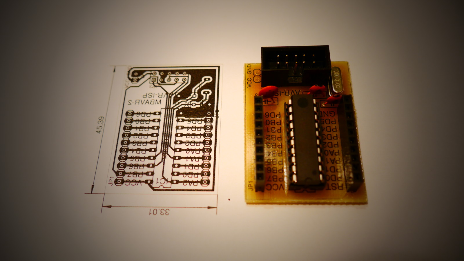
This is a quick how-to guide of making a minimalist development boards for MCU of tinyAVR, like ATiny2313 or ATiny4313. MBAVR-2 is a second project in series of MBAVR family home-made boards in order to create an nice environment for rapid development. All I did, I did at home. I used toner transfer technique for both layers. The process of creating PCB description layer turned out quite straight forward. Generally, I’m pleased with the results.
Intro
The project goal was the same as of previous version – to create minimalist development board that will:
- base on signle-layer PCB layout,
- include only through hole parts,
- expose AVR ISP socket (JP3) for USBasp programmer,
- make all GPIO pins available on the PCB via headers (JP1, JP2)
- contain MCU socket and extra power connector (JP4).
Designing complex development boards is often overkill, especially when you want it small size. On the board shown here, I’m only using the features turned out to be handy for what I’m using in my projects. I focused on design that in my opinion is possibly a simplest, smallest, and cheapest.
List of elements:
- PCB,
- microcontroller (ATtiny2313/ATtiny4313),
- DIL-20 socket,
- two pin headers 10×1,
- and one pin header 2×1.
- crystal 10Mhz (according to manual it’s optimal value for both 3.3V and 5.0V)
- two capacitors 24pF,
- capacitor 10nF (decoupling capacitor).
Diagram Circuit
Additional information about schematic and PCB can be found in eagle project which is attached to this article as a zip file.


